
On-Chip Amplifier 2.


OD
OS
RD

R
SW
Output
Node
Output
Transistor
Reset
Transistor
Summing
Well

+5V
0V
-5V
+10V
0V


R
SW


--end of
serial register


Vout
Vout
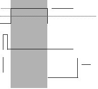
The charge
is then transferred onto the Summing Well. Vout is now at the
‘Reference level’
There is now a wait of up to a few tens of
microseconds while external circuitry measures
this ‘reference’ level.
